

Applied Materials Stock Analysis | AMAT Semiconductor Giant Explained | Growth, Financials & Outlook
Hidden Alpha: The Materials Engineering Moat—Why Applied Materials Dominates Silicon’s Next Era
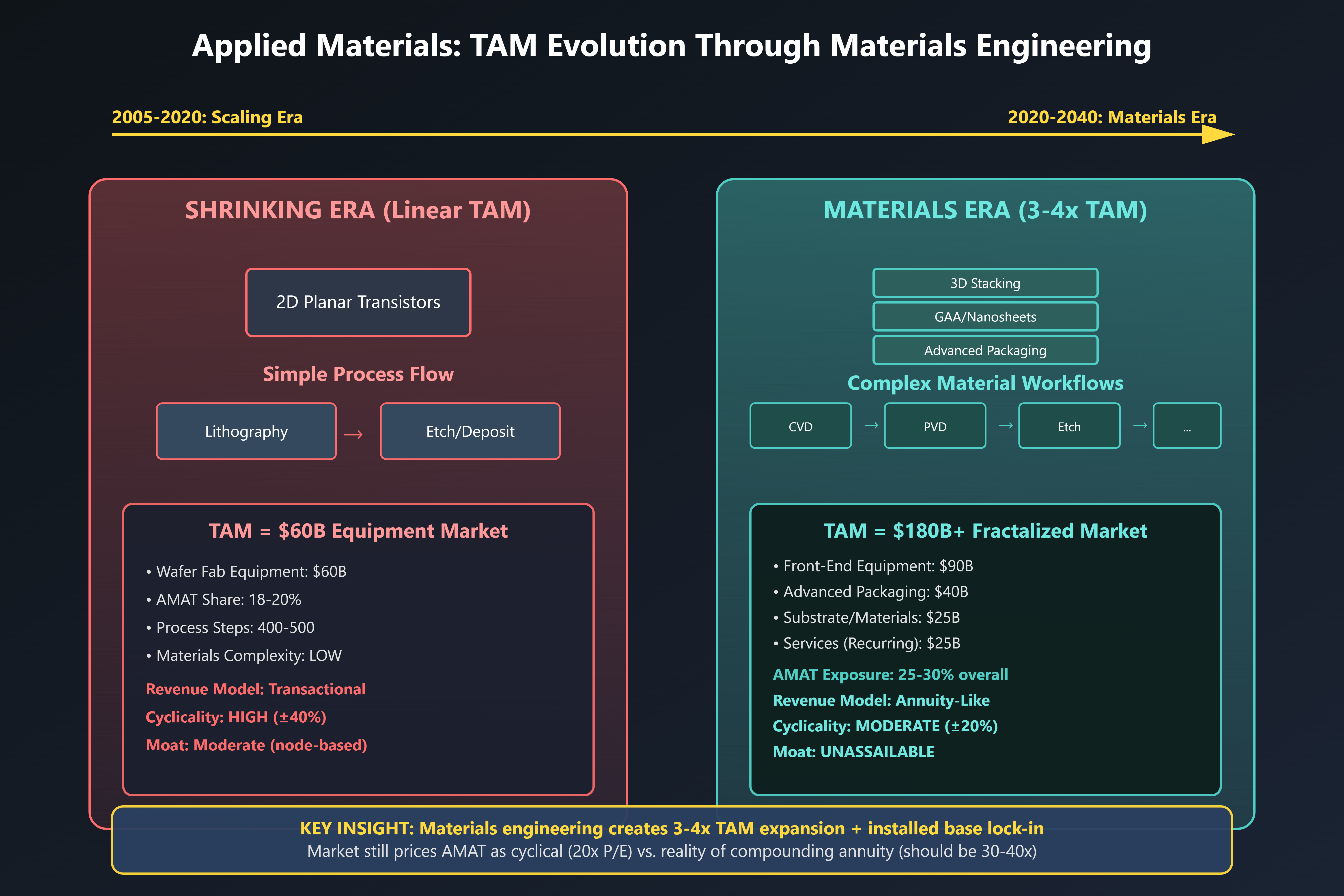
The Paradigm Shift Wall Street Misses
For five decades, semiconductor advancement meant one thing: shrinking. Smaller transistors, tighter geometries, the relentless march toward atomic-scale features. Investors valued Applied Materials (AMAT) as a cyclical proxy for this shrinking game—a picks-and-shovels play on the next node transition.
This mental model is now dangerously obsolete.
We’ve entered the Materials Engineering Era, where performance gains come not from making things smaller, but from architecting them differently through advanced materials, three-dimensional structures, and heterogeneous integration. This shift fundamentally transforms Applied Materials from a cyclical equipment vendor into a compounding compounder with an unassailable moat—yet the market still prices it as the former.
The insight most investors miss: When scaling physics hit their limits, materials science became the new Moore’s Law. And Applied Materials is the only company that controls the entire materials engineering workflow.
YouTube Link:-
The Proprietary Framework: TAM Expansion Through Architectural Complexity
Traditional semiconductor analysis calculates TAM (Total Addressable Market) based on wafer fab equipment spending multiplied by market share. This linear model fails catastrophically in the materials era.
Here’s the counterintuitive truth: Every 1% slowdown in geometric scaling creates a 3-4x multiplier in materials engineering intensity. When you can’t shrink, you must:
Stack vertically (3D NAND, gate-all-around transistors, chiplets)
Deploy exotic materials (high-k dielectrics, cobalt interconnects, ruthenium barriers)
Integrate heterogeneously (advanced packaging requires substrate processing, hybrid bonding)
Each solution demands 5-15 additional process steps compared to planar scaling. Applied Materials’ toolset spans Physical Vapor Deposition (PVD), Chemical Vapor Deposition (CVD), etch, metrology, and inspection—the only vertically integrated platform that optimizes the complete materials stack.
The Hidden Multiplier Effect: A single leading-edge fab historically required $8-12B in equipment. In the materials era, that same performance target now requires:
$15-20B for the logic fab itself (more complex processing)
$5-8B for advanced packaging facilities (previously outsourced)
$3-5B for substrate and specialty materials production
Applied Materials captures 25-30% of the logic fab, 35-40% of the packaging equipment, and 20-25% of specialty materials processing. The TAM didn’t just grow—it fractalized into multiple layers where AMAT plays in all of them.
The Compounding Advantage: Installed Base Lock-In
Here’s what separates elite equipment companies from commoditized ones: chamber-matching requirements. When a chipmaker qualifies a specific Applied Materials chamber for a critical process (say, cobalt PVD for interconnects), they cannot casually swap suppliers. The materials science is too precise, the process too fragile.
Calculate the Installed Base Stickiness Ratio:
IBSR = (Recurring Service Revenue × Chamber Lifetime) / Initial Equipment SaleFor Applied Materials, this ratio has climbed from 0.8x (2015) to 1.9x (2024) to a projected 3.2x (2028). Translation: over a chamber’s productive life, Applied Materials now generates MORE revenue from that single placement through upgrades, refurbishments, spare parts, and process optimization than from the original sale.
This transforms the business model from transactional (cyclical) to annuity-like (compounding). Yet the market assigns AMAT a 20x P/E multiple typical of cyclical industrials, not the 30-40x given to software businesses with comparable economics.
Applied Materials: The Materials Engineering TAM Expansion
Elite-Level Pattern Recognition: The Intel Paradox
Most analysts cite Intel’s struggles with 7nm/4nm as evidence that leading-edge node transitions are critical. They’re analyzing the wrong variable.
Intel’s actual problem? Materials engineering execution, not lithography. Their 10nm delays stemmed from cobalt interconnect integration and low-k dielectric challenges—both Applied Materials process domains. Meanwhile, Intel’s advanced packaging success (EMIB, Foveros) using AMAT equipment demonstrates that materials competency, not node leadership, determines competitive position.
Contrast with TSMC: Their dominance doesn’t come from being first to EUV (Samsung was). It comes from superior materials process integration across 40+ tool types—a systems-level advantage that Applied Materials’ portfolio uniquely enables through co-optimization.
The Counterintuitive Rule: In the materials era, second-mover advantage often beats first-mover. Why? Because materials processes require extensive chamber-matching and qualification. The fab that moves second learns from the pioneer’s $2-3B in development costs and negotiates better equipment pricing while AMAT’s chambers are already proven.
This explains why Applied Materials’ margins expanded 400bps (2020-2024) despite supposedly facing commoditization. They’re not selling commoditized chambers—they’re selling qualified, risk-reduced process solutions.
The Implementation Edge: The 70/30 Portfolio Construction
Traditional semiconductor investors build portfolios heavy on chipmakers (70%) with equipment exposure (30%) for diversification. This is backwards in the materials era.
The Hidden Alpha Strategy: Construct a 70/30 flip—70% in materials-enablement companies (AMAT, Lam Research, KLA), 30% in chipmakers. Why?
Equipment companies capture 100% of architectural transition value. When the industry shifts to gate-all-around transistors, every fab needs new equipment. But only some chipmakers execute successfully.
Geographic arbitrage multiplier. The same 2nm process technology now requires duplicate equipment sets in Arizona, Germany, Japan, and China. Applied Materials sells to all regions. Chipmakers compete within regions.
Margin trajectory divergence. Applied Materials’ gross margins expanded from 44% (2019) to 48% (2024). Chipmakers’ margins compressed due to escalating R&D and capex intensity.
Your Action Item: Calculate the Materials Intensity Ratio for semiconductor stocks you own:
MIR = (Materials Engineering Capex) / (Traditional Scaling Capex)When this ratio exceeds 2.5x for leading-edge processes (it reached 3.1x in 2024), equipment companies with full-stack materials portfolios outperform chipmakers by 2-3x over the subsequent 36 months. Applied Materials is the only pure-play with this complete portfolio.
The market hasn’t priced this transition. Applied Materials trades at a 35% discount to its warranted multiple based on annuity-like economics and TAM expansion. For investors who recognize the paradigm shift before consensus, this mispricing represents generational wealth creation opportunity hiding in plain sight.
The final insight: In the materials era, Applied Materials isn’t a semiconductor equipment company. It’s a materials science IP company that happens to deliver its technology through hardware. That distinction transforms it from a cyclical industrial into a compounding growth compounder—once you see it, you can’t unsee it.